HOYA’s EUV Photomask Blanks: The Key to Next-Generation Semiconductors
Discover how HOYA Electronics’ critical EUV photomask blanks enable the advanced semiconductors powering our digital world, from AI to 5G, pushing the limits of technology with EUV lithography.
In today’s interconnected world, we navigate life through a constellation of digital devices. From smartphones connecting us globally to the complex algorithms driving Artificial Intelligence and the high-speed networks enabling 5G, sophisticated technology is woven into the fabric of modern existence. Yet, beneath the sleek interfaces lies a world of microscopic complexity: the semiconductor chip. Manufacturing these tiny powerhouses, the brains of all electronics, demands extraordinary precision and relies on foundational components often unseen by the end-user. As technology demands smaller, faster, and more powerful chips, the industry faces significant hurdles, pushing innovation to its limits.
Meeting this escalating demand requires overcoming fundamental physical barriers in chip manufacturing, particularly when shrinking features below the 7-nanometer threshold. This is where cutting-edge technology like Extreme Ultraviolet (EUV) lithography becomes essential, allowing for unprecedented miniaturization. However, EUV technology itself depends critically on highly specialized components.
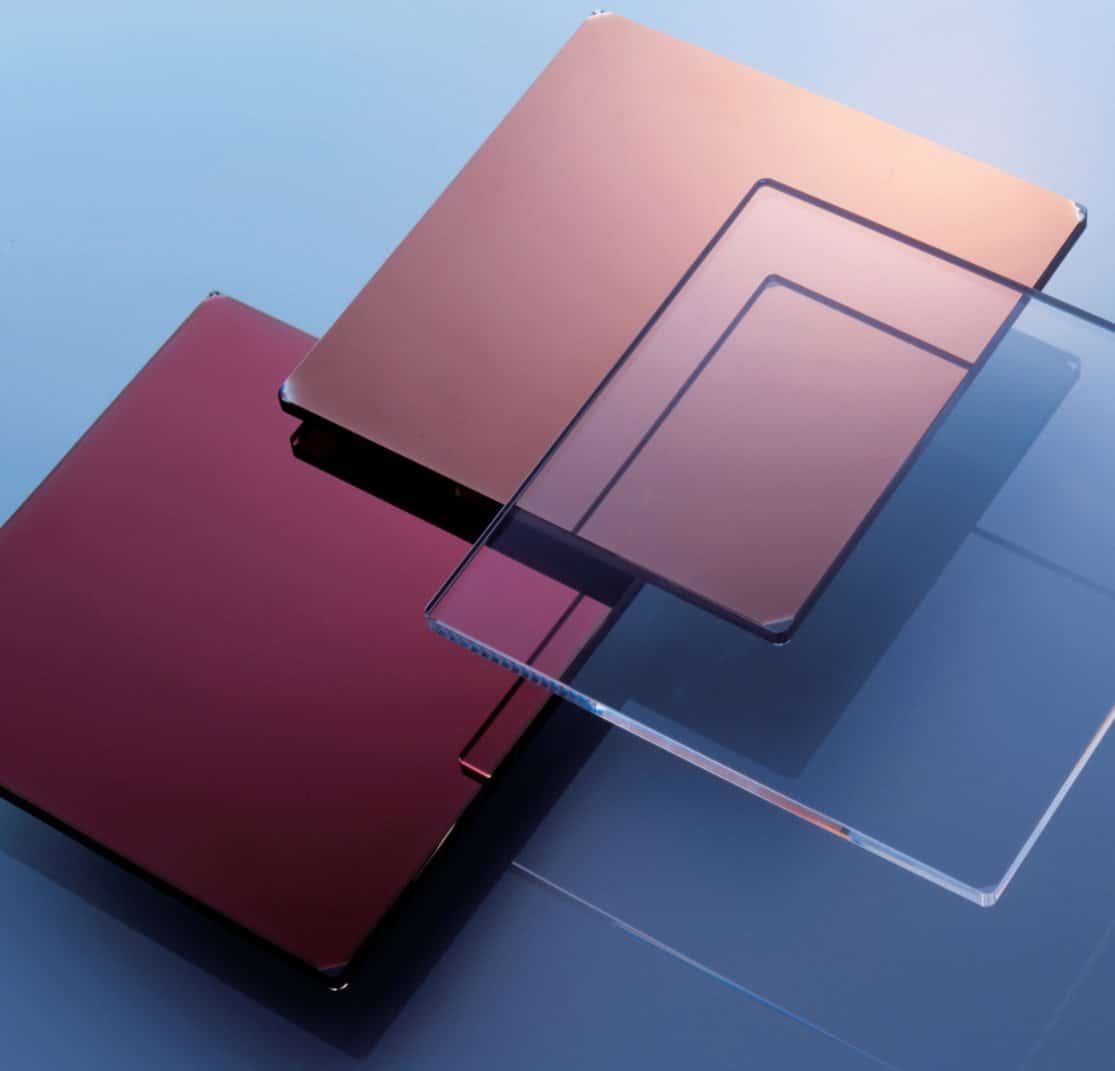
HOYA Electronics is a global leader supplying one of the most crucial yet least known components: the photomask blank. HOYA provides the pristine starting material upon which chip designs are patterned. The revolutionary EUV process involves creating incredibly complex EUV photomask blanks, which are multi-layered structures featuring near-perfect flatness and specialized coatings designed to reflect EUV light precisely. These blanks act as the foundation for the stencils (photomasks) that imprint circuit designs onto silicon wafers. Without reliable, high-quality EUV photomask blanks, mass production of the most advanced chips would not be possible.
“The relentless pace of innovation means the technologies we develop today, like our advanced EUV blanks, directly enable the devices and capabilities that will shape tomorrow’s world,” remarked Geoffrey Maroun Akiki, HOYA IT Segment Company President. HOYA Electronics, through decades of expertise and continuous innovation, provides these indispensable materials, ensuring chipmakers can leverage EUV technology effectively.
The journey is remarkable—transforming raw quartz through meticulous purification and polishing processes into a highly engineered photomask blank, precisely measuring 152 by 152 by 6.35 millimeters. Getting from this essential starting point, which must meet incredible standards of flatness and purity, to the powerful processor in your device is a testament to intricate global collaboration and relentless innovation. HOYA Electronics’ role in providing these foundational materials is critical. By mastering the production of conventional and cutting-edge EUV photomask blanks, the company is enabling the entire semiconductor ecosystem to push forward. This commitment underpins the future of high-performance computing, advanced AI, and next-generation communications, ensuring the seemingly invisible building blocks of our digital world continue to drive progress for years to come.
Find out more about Economy 4.0 Campaign


